配線工程
配線工程またはバックエンド(back end of line、BEOL)とは、半導体製造における2番目の工程であり、それぞれのデバイス(トランジスタ、キャパシタ、抵抗など)がメタル層によって配線される。 配線材料として以前はアルミニウム配線が使われていたが、その後銅配線に置き換わった[1] 。 ウェハー上に最初のメタル層が成膜されてからがBEOLである。
.svg.png.webp)
BEOL(メタル層)とFEOL(デバイス)
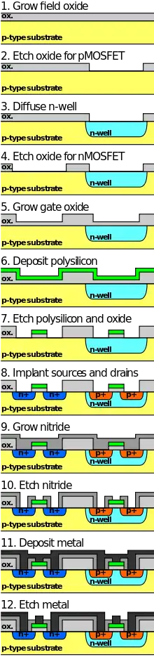
CMOS製造プロセス
BEOLのステップ:
引用
- Karen A. Reinhardt and Werner Kern (2008). Handbook of Silicon Wafer Cleaning Technology (2nd ed.). William Andrew. p. 202. ISBN 978-0-8155-1554-8
参考文献
- “Chapter 11: Back End Technology”. Silicon VLSI Technology: Fundamentals, Practice, and Modeling. Prentice Hall. (2000). pp. 681–786. ISBN 0-13-085037-3
- “Chapter 7.2.2: CMOS Process Integration: Backend-of-the-line Integration”. CMOS: Circuit Design, Layout, and Simulation. Wiley-IEEE. (2010). pp. 199–208 [177–79]. ISBN 978-0-470-88132-3
This article is issued from Wikipedia. The text is licensed under Creative Commons - Attribution - Sharealike. Additional terms may apply for the media files.